Semiconductor Device Simulation
Computer Architecture Group
Departamento de Electronica e Computación - USC
Spintronics

The main objective in our work in the field of the spintronics is the development of analytical and numerical models for the simulation of spintronic devices based on diluted magnetic semiconductors (DMS). There is growing interest within the scientif community in the use of electron spin as an information carrier. In particular, several research groups have been studying magnetic semiconductors, observing a large amount of exotic properties, such as the giant magnetoresistance (GMR) and magneto-optical properties, originating from the concurrence of ferromagnetic and semiconductor properties. Currently, most of the research related to magnetic semiconductors is focused on semiconductor alloys that incorporate magnetic impurities which substitute atoms from the crystal lattice. Considering the ease with which structures based on DMS can be grown using current techniques, such as molecular beam epitaxial growth (MBE), there is a broad interest in the study of multilayer and thin layer structures based on II-VI and III-V compounds like ZnO and GaAs.
In this task we have focused on the development of analytical and numerical models for the simulation of these kinds of devices. We have divided the work into two different stages: (i) the study of atomistic models for the simulation and characterisation of these new materials and (ii) the design of simulation techniques which allow the integration of the results coming from the previous stage with the study of the transport properties and magneto-optical properties in DMS based devices.
Simulation of magnetic semiconductor materials
The study of the models that allow a good characterisation of these new materials is essential for the development of suitable models to allow the prediction of the behaviour of the devices based on DMS. For this reason, firstly we intend to analyse the functionality of models based on techniques such as the empirical tight binding (ETB), the density functional theory (DFT) and others that are starting to produce good results for II-VI and III-V semiconductors. The obtained characterisation in terms of band structures, density of states and electron and hole densities will be then employed in the development of transport models for magnetic materials.


Development of analytical and numerical models for spintronic devices
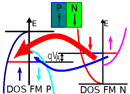
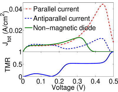
Once the materials have been properly characterised, the aim is to develop numerical and analytical models to simulate devices based on DMS, following multiphysics techniques that allow the integration of atomistic models with the traditional numerical methods for simulating electronic devices. The objective is to simulate heterostructures based on GaAs and ZnO, with magnetic impurities, to study the behaviour of the tunnel magneto-resistance (TMR) and the magnetic and optic properties and their dependence on temperature, high degeneracy effects and the influence of magnetic and electric fields. These results will be validated against experimental results currently available to verify the correct operation of the simulator. Then it will be employed to predict the behaviour of other architectures.
- Devices
- III-V MOSFET
- finFET
- Solar Cells
- Spintronics
- Simulation Tools
- Drift-Diffusion
- Monte Carlo
- Finite Elements
- Synopsys TCAD Sentaurus
- Contact
- People
- Contact us