Semiconductor Device Simulation
Computer Architecture Group
Departamento de Electronica e Computación - USC
3D Simulation of III-V implant free MOSFET

With the scaling of the CMOS technology towards the sub-22 nm generation, silicon-channel conventional and novel MOSFET architectures face difficulties to meet the performance requirements. Therefore, intensive research is underway to replace the Si channel with other high-mobility semiconductor which can deliver significant performance improvement. MOSFETs with Ge channels for p-channel applications or compound semiconductors for n-channel applications are now a widely accepted option for overcoming the performance limitations inherent to the low mobility of Si. Recent developments such as the demonstration of a high-k and suitable epitaxial layer structures have substantially improved the prospect for the introduction of III–V MOSFETs for high-performance low-power CMOS applications.
III–V n-channel MOSFETs in combination with high-performance p-channel Ge transistors are becoming serious candidates for co-integration in dual channel CMOS platforms, which may have unique advantages in regard to RF, switching and power control functions. With the scaling of silicon MOSFETs to nanometre dimensions, the intrinsic parameter variation introduced mainly by discreteness of charge and matter has become a major bottleneck to scaling and integration. Therefore, it is extremely important to reduce the variability provoked by the different sources of intrinsic fluctuations, which being inherent to the devices cannot be eliminated by improvements in the fabrication process.


Device Structure and Calibration
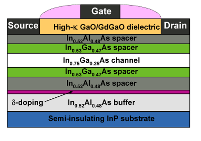
An example of the devices we work with is shown in Figure 1. It shows the structure of an In0.75Ga0.25As enhancement mode MOSFETs with implant free source/drain regions. The MOSFET structure is grown on an InP substrate and consists of a 49 nm In0.52Ga0.48As buffer layer and a Si delta-doping layer heavily doped. The In0.75Ga0.25As channel layer is sandwiched between In0.53Ga0.47As embed layers. The high-mobility channel forms a quantum well with energy barriers comparable to the supply voltages at and beyond the 22 nm node. In this way, the carriers are well confined to the channel, providing ultra-thin body like scaling performance. Finally, an amorphous Ga2O3/GdGaO dielectric stack is used to separate a metal gate.
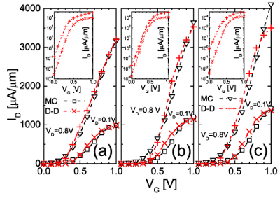
These devices have been studied using a 3D drift-diffusion simulator that has been calibrated against ID-VG characteristics obtained from Monte Carlo simulation results at low and high drain biases, as shown in Figure 2 for three gate lengths of 30, 20 and 15 nm, respectively.
Threshold voltage variability
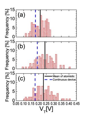
One of the major sources of statistical variability are the random discrete dopants in the active region of the transistors. For example, to investigate the threshold voltage variations in the IF MOSFETs introduced by the random discrete dopants in the delta-doped layer, a random distribution of dopants is generated from the continuous doping profile. We have generated statistical samples of 100 microscopically different transistors. The distributions of threshold voltage at drain bias of 0.1 V are presented in Figure 3 for 30 (a), 20 (b) and 15 (c) nm gate length devices.
- Devices
- III-V MOSFET
- finFET
- Solar Cells
- Spintronics
- Simulation Tools
- Drift-Diffusion
- Monte Carlo
- Finite Elements
- Synopsys TCAD Sentaurus
- Contact
- People
- Contact us