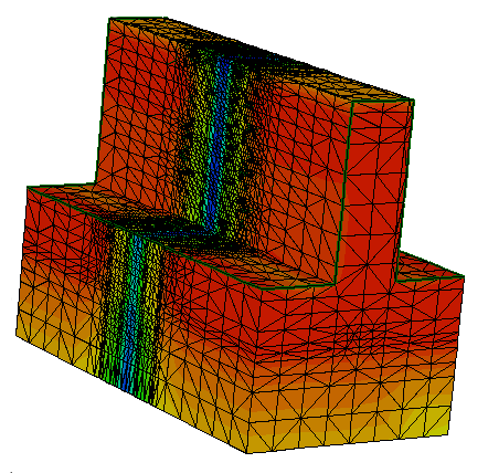
Semiconductor Device Simulation
Computer Architecture Group
Departamento de Electronica e Computación - USC
Process and Device Simulation Tools

Technology Computer-Aided Design (TCAD) refers to the use of computer simulations to develop and optimize semiconductor processing technologies and devices. Synopsys TCAD offers a comprehensive suite of products that includes industry leading process and device simulation tools, as well as a powerful GUI-driven simulation environment for managing simulation tasks and analyzing simulation results. The TCAD process and device simulation tools support a broad range of applications such as CMOS, power, memory, image sensors, solar cells, and analog/RF devices. In addition, Synopsys TCAD provides tools for interconnect modeling and extraction, providing critical parasitic information for optimizing chip performance.
Process simulation

Sentaurus Process is an advanced 1D, 2D and 3D process simulator for developing and optimizing silicon semiconductor process technologies. It is a new-generation process simulator for addressing the challenges found in current and future process technologies. Equipped with a set of advanced process models, which include default parameters calibrated with data from equipment vendors, Sentaurus Process provides a predictive framework for simulating a broad range of technologies from nanoscale CMOS to large-scale high-voltage power devices. Sentaurus Process is part of a comprehensive suite of core TCAD products for multi-dimensional process, device, and system simulations, embedded into a powerful user interface.
Benefits:
- Fast prototyping, development, and optimization of a broad range of technologies with comprehensive physics-based process modeling capabilities.
- Enhance device performance by optimization of thermal and mechanical stress in process structures with stress history.
- Provides insights into advanced physical phenomena through self-consistent multi-dimensional modeling capabilities.
Device simulation
Sentaurus Device is an advanced multidimensional device simulator capable of simulating electrical, thermal, and optical characteristics of silicon-based and compound semiconductor devices. Sentaurus Device is a new-generation device simulator for designing and optimizing current and future semiconductor devices. Sentaurus Device is a general purpose device simulation tool which offers simulation capability in the following broad categories:
- Conventional and Deep Submicron CMOS Technologies: Sentaurus Device can simulate all silicon and strained silicon technologies including Silicon Germanium (SiGe) pockets or other external stress sources. Advanced numerical capabilities can capture hot carrier effects, non-local and quantum effects for advanced applications. Sentaurus Device’s 3D simulation capability can simulate narrow width effects in deep submicron devices, parasitic channel effect in shallow trench isolation and floating body effect in SOI structures.
- Compound Semiconductor Technologies: Sentaurus Device can simulate advanced quantization models including rigorous Schrödinger solution and complex tunneling mechanisms for transport of carriers in heterostructure devices like HEMTs and HBTs made from, but not limited to, GaAs, InP, GaN, SiGe, SiC, AlGaAs, InGaAs, AlGaN and InGaN.
- Optoelectronic Devices: Sentaurus Device has the capability to simulate the optoelectronic characteristics of semiconductor devices like CMOS image sensors, solar cells, and lasers. Options within Sentaurus Device also allow for rigorous solution of the Maxwell’s wave equation using FDTD methods.
- Power Electronic Devices: Sentaurus Device is the most flexible and advanced platform for simulating electrical and thermal effects in a wide range of power devices such as IGBT, power MOS, LDMOS, thyristors, and high-frequency high-power devices made from wide band-gap material like GaN and SiC.
- Monte Carlo Device Simulation: Sentaurus Device offers a rigorous solution of Boltzmann’s equation using robust and computationally efficient full band ensemble Monte Carlo methods for very small gate length devices.
- Memory Devices: With advanced carrier tunneling models for gate leakage and trapping de-trapping models, Sentaurus Device can simulate any floating gate device like SONOS and flash memory devices including devices using high-K dielectric.
- Radiation Effects: The impact of radiation on semiconductor device operations can be studied with Sentaurus Device. Both single event effects, which include single event upset (SEU) and single event transient (SET), and total ionization dose (TID) effects can be simulated.
- Novel Semiconductor Technologies: Advanced physics and the ability to add user-defined models in Sentaurus Device allow for investigation of novel structures made from new material.
Benefits:
- Explore new device concepts for which fabrication processes are not yet defined
- Characterize electrical, thermal and optical behavior of semiconductor devices for fast prototyping, development and optimization of their performance
- Shorten development time by supplementing experimental data with deep physical insight from simulation
- Study sensitivity of device characteristics to process variation for optimizing parametric yields
- Devices
- III-V MOSFET
- finFET
- Solar Cells
- Spintronics
- Simulation Tools
- Drift-Diffusion
- Monte Carlo
- Finite Elements
- Synopsys TCAD Sentaurus
- Contact
- People
- Contact us