Semiconductor Device Simulation
Computer Architecture Group
Departamento de Electronica e Computación - USC
finFET

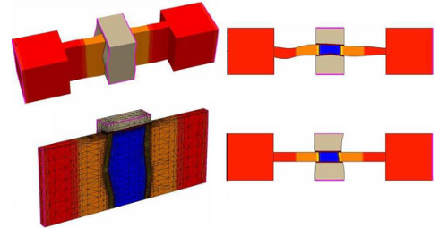
Various novel thin-body architectures have been proposed to tackle the degradation in performance observed in the conventional, bulk 22 nm technology and beyond. FinFETs are among the strongest contenders to satisfy the requirements imposed by ITRS and continue the scaling. As the ITRS 2010 suggests, accurate physical modelling of carrier transport and correct description of 3D geometry (Fig. 1) is necessary for the prediction of device performance and optimisation of its design. For the current and near-future device dimensions, such physical modelling can be achieved via the ensemble Monte Carlo (MC) method. However, this technique is computationally very expensive for complex 3D geometries and its use in all working conditions is inefficient. We have adopted a multi-model approach to the simulations adopting simpler transport models where they are enough for an accurate reproduction of the device characteristics.
As a model device to test the simulations we have used a design based on the description given in published papers of a 25 nm gate length FinFET with a silicon body 30 nm high and 12 nm wide. The doping profile was calibrated to match the experimental data in the subthreshold region as shown in the figure.
- Devices
- III-V MOSFET
- finFET
- Solar Cells
- Spintronics
- Simulation Tools
- Drift-Diffusion
- Monte Carlo
- Finite Elements
- Synopsys TCAD Sentaurus
- Contact
- People
- Contact us