Semiconductor Device Simulation
Computer Architecture Group
Departamento de Electronica e Computación - USC
Solar Cells

The possibility of using a-Si:H in the production of PV modules on a large scale caused in recent decades a great interest in modeling and understanding of the electronic processes that occur in devices made with this material. The main advantages to use thin film a-Si:H modules include enhanced power output under high temperature conditions, due to smaller temperature coefficients, greater absorption of diffuse radiation, lower energy payback time and low fabrication costs. Grupo T-Solar is an independent photovoltaic (PV) electricity producer and manufacturer of amorphous hydrogenated-silicon (a-Si:H) thin film modules. T-Solar Global S.A., (T-Solar) subsidy of Grupo T-Solar, has installed a highly automated a-Si:H PV module factory in Orense, Spain with a production capacity of around 45 MWp per year.
Due to the complexity of the involved physical phenomena has become imperative to use numerical simulation to solve the physical equations that describe the operation of such devices. Realistic modeling of solar cell operation, i.e. the resolution of the full set of physical equations that describe the behavior of a solar cell, should help in understanding the physical processes that occur during cell operation and allow determining the mechanisms that limit their performance. Device simulation is a promising tool to improve module performance and to reduce manufacturing costs. Therefore, our group and T-Solar R&D deparment have started to perform two dimensional simulations of a-Si:H solar cells using the software package Sentaurus TCAD (Synopsys Inc.).

Single junction pin a-Si:H solar cells
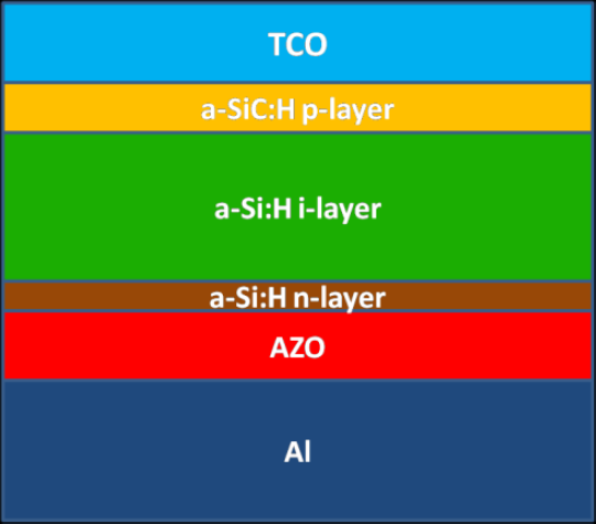
The structure of the a-Si:H solar cell that we simulate is TCO/p-type a-SiC:H/i-layer a-Si:H/n-type a-Si:H/AZO/Al. For the baseline structure, TCO is tin oxide doped with fluorine (SnO2:F). We use a-SiC:H for the p-layer because of its wider band gap and higher conductivity in comparison to a-Si:H that results in a higher built-in potential and allowing more light to reach the absorber layer and therefore, improving the open circuit voltage as well as short circuit current. In the simulation, the p-type layer is doped with boron and the n-type layer and the intrinsic layer with phosphorus (latter basically to define the i-layer conductivity due to intrinsic doping). The function of the p and n doped layers is to establish an electric field over the “nominally” undoped photo absorbing i-layer and to provide a good electrical contact to the end terminals on either side. The back electrode is made such that it acts as an optical mirror, using reflective metals such as Al. We introduce a reflection-enhancing dielectric layer such as Al-doped zinc oxide (AZO) between the silicon and the metal electrode.
To simulate accurately the electrical and optical properties of a-Si:H solar cell, a proper description of the density of states (DOS) distribution as a function of energy is of major importance. The standard model of the DOS distribution of a.Si:H consists of a parabolic conduction band (CB), a parabolic valence band (VB), an exponentially decaying conduction band tail (CBT) and exponentially decaying valence band tail (VBT). Two equal distributions of states around the midgap that are separated from each other by a correlation energy (U), represent the defect states related to Si dangling bonds (DB+/0 and DB0/-), to consider the amphoteric character of the defect states existing in a-Si:H. The a-Si:H band gap is characterized by a continuous density of allowed states that in its entirety contributes to the net R-G rate.

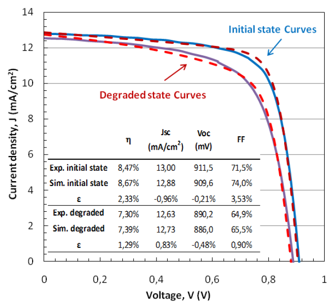
We achieve a good agreement between the measured and simulated J-V characteristics of a typical small (1cm2) solar cell prepared with a special procedure in the T-Solar production line. Important model parameters for the open circuit voltage (Voc) are the mobility gap of the i-layer and the activation energy of the p-layer. The influence of the mobility gap and the effective density of extended states in the i-layer is related to their impact on the maximum possible separation of the quasi-Fermi levels in the i-layer due to optical carrier generation. Since Voc also depends on the carrier recombination in the device, a strong influence of the band tail parameters and the defect density on the Voc is observed. The short circuit current density (Jsc) is sensitive to the optical parameters of all layers and to the irradiance level. The fill factor (FF) of the solar cell under standard AM1.5 illumination is sensitive to those parameters that determine the conductivity of the layers such as the activation energy of the p-layer and the intrinsic layer. Due to the presence of weak Si-Si bonds and the relative ease of diffusive motion of hydrogen, metastable dangling bonds can be created in addition to the initially present dangling bond density by the breaking of these weak bonds. This effect is known as the Staebler-Wronski effect. The creation of metastable defects is driven by the release of energy due to electron-hole recombination events, and is thus enhanced by illumination of the material. The increased dangling bond density reduces the electric field within the intrinsic layer of the cell and enhances the recombination losses in the cell, by which the cell performance deteriorates.
Tandem solar cells

Solar cell texturization
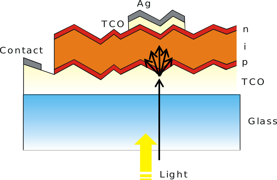
The main objectives of the photovoltaic industries are to mimize costs and to increase the cell eficiency. Some of the strategies to increase the use of the light in the intrinsic layer are to reduce the optic losses in the non active regions of the cell and increasing the light confinement.
Using a back contact with good mirror behaviour, reducing the absortion in the p and n layers and also using a highly transparent front contact are techniques to reduce the optical losses. Also increasing the light catching by anti-reflection coatings and the light trapping by the the use of interface texturization increases the total current in the device
- Devices
- III-V MOSFET
- finFET
- Solar Cells
- Spintronics
- Simulation Tools
- Drift-Diffusion
- Monte Carlo
- Finite Elements
- Synopsys TCAD Sentaurus
- Contact
- People
- Contact us